Home
› Full Adder Logic Diagram And Truth Table / Half Adder Logic Diagram And Truth Table - Wiring Diagram Schemas - Full adder circuit construction is shown in the above block diagram, where two half adder circuits added together with a or gate.
Full Adder Logic Diagram And Truth Table / Half Adder Logic Diagram And Truth Table - Wiring Diagram Schemas - Full adder circuit construction is shown in the above block diagram, where two half adder circuits added together with a or gate.
Full Adder Logic Diagram And Truth Table / Half Adder Logic Diagram And Truth Table - Wiring Diagram Schemas - Full adder circuit construction is shown in the above block diagram, where two half adder circuits added together with a or gate.. Truth table with three inputs. I drew the truth i think v hav to use full adder here.is tht? Here is the logic diagram: The truth table is shown. Full adder definition, block diagram, truth table, circuit diagram, logic diagram, boolean expression and equation are discussed.
Full adder combinational logic circuits electronics tutorial. Write down the truth table for each part in the labwork below 2. F = 1 if and only if there is a 0 to the left of a 1 in the input. Truth table with three inputs. Full adder is a combinational device.
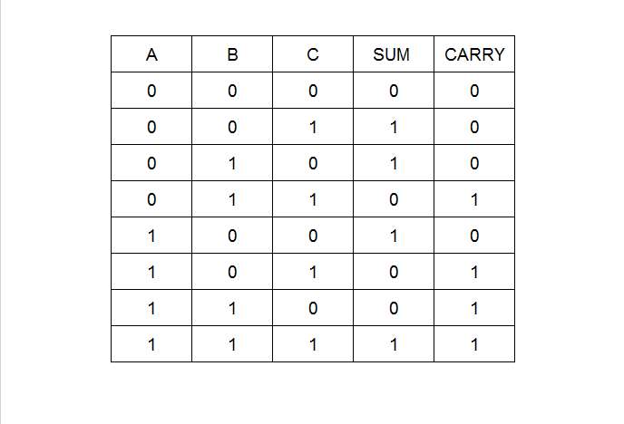
Combinational Circuits | "ASPIRANTS" from gs-blog-images.s3-ap-southeast-1.amazonaws.com F = 1 if and only if there is a 0 to the left of a 1 in the input. The sum 's' is produced in two steps the implementation of larger logic diagrams is possible with the above full adder logic a simpler symbol is mostly used to represent the operation. Figure shows the truth table of a full adder circuit showing all possible input combinations and corresponding outputs. The possible outputs combinations are 2^n. Full adder working principle circuit diagram etc. Truth table with three inputs. Full adders are complex and difficult to implement when a full adder can be formed by logically connecting two half adders. Draw pin connection diagram and function table of the binary adder 74ls83 ic using.
The truth table is shown.
Here is the logic diagram: An adder is a digital circuit that performs addition of numbers. Full adder is a combinational logic circuit used for the purpose of adding two single bit numbers with a carry. The truth table is shown. Where s is the sum and c is the carry out. A full adder can be implemented using two half adders as shown in the 1. In the above image, instead of block diagram, actual symbols are shown. **draw truth table and logic diagram of full subtractor.** the full subtractor is a combinational circuit with three inputs a, b and bin and two outputs d and bo. Step by step procedure to design full adder block diagram,truth table,k map and logic circuits please visit the links below for. The truth table and corresponding karnaugh maps for it. Logic diagrams are diagrams in the field of logic, used for representation and to carry out certain types of reasoning. Draw the logic diagram for a circuit that implements the function in question 7. They are also used in other parts of the processor, where they are used to calculate addresses, table indices.
Adders are classified into two types: In these circuits there are n input variables obtained from an external source are of binary type. Where s is the sum and c is the carry out. Full adders are complex and difficult to implement when a full adder can be formed by logically connecting two half adders. When led glows it represents logic high (1), during off condition led represents logic.
Combinational Circuit - Adder Circuits - NotesforMSc from notesformsc.org Full adder working principle circuit diagram etc. Which is add a 3 bit data and generate output carry and sum. When led glows it represents logic high (1), during off condition led represents logic. And the corresponding truth table: Figure shows the truth table of a full adder circuit showing all possible input combinations and corresponding outputs. Truth table with three inputs. The following is a block diagram that shows the implementation of a full. Draw the truth table for a logic function that takes a three bit binary number and produced an output that is 0 for even parity and 1 for odd parity.
Even though this is a simple adder and can be used to add unrestricted bit length numbers, it is however not very efficient.
In these circuits there are n input variables obtained from an external source are of binary type. A full adder circuit is central to most digital circuits that perform addition or subtraction. Draw the logic diagram for a circuit that implements the function in question 7. A, b and cin, which add three input binary digits and generate two binary outputs i.e. The arithmetic circuitry in most processors is carried out by a unit called the arithmetic logic unit (alu. It is a type of digital circuit that performs the operation of additions of two number. Logic diagrams are diagrams in the field of logic, used for representation and to carry out certain types of reasoning. And the corresponding truth table: We can see that the output s is an exor between the input a and the though the implementation of larger logic diagrams is possible with the above full adder logic a simpler symbol is mostly used to represent the operation. Truth tables offer a simple and easy to understand tool that can be used to determine the output of any logic gate or circuit for all input combinations. Full adder circuit construction is shown in the above block diagram, where two half adder circuits added together with a or gate. In the above image, instead of block diagram, actual symbols are shown. Here is the logic diagram:
Figure shows the truth table of a full adder circuit showing all possible input combinations and corresponding outputs. When a logic gate has only two inputs, or the logic circuit to be analyzed has only one or two gates, it is fairly easy to remember how a. The arithmetic circuitry in most processors is carried out by a unit called the arithmetic logic unit (alu. In these circuits there are n input variables obtained from an external source are of binary type. Half adder and full adder circuit electronics engineering study.
1. Adder A. Construct The Truth Table Of A 1-bit F... | Chegg.com from d2vlcm61l7u1fs.cloudfront.net The following is a block diagram that shows the implementation of a full. The truth table is shown. Logic diagrams are diagrams in the field of logic, used for representation and to carry out certain types of reasoning. Where s is the sum and c is the carry out. Full adder using nor logic: And the corresponding truth table: The logic gates present in it acts based upon the signals. Truth tables offer a simple and easy to understand tool that can be used to determine the output of any logic gate or circuit for all input combinations.
Draw the truth table for a logic function that takes a three bit binary number and produced an output that is 0 for even parity and 1 for odd parity.
Full adder circuit construction is shown in the above block diagram, where two half adder circuits added together with a or gate. Here is the logic diagram: The truth table and logic diagram of a 1 bit full adder is shown below. **draw truth table and logic diagram of full subtractor.** the full subtractor is a combinational circuit with three inputs a, b and bin and two outputs d and bo. Which is add a 3 bit data and generate output carry and sum. In order to arrive at the logic logic circuit diagram of full adder. Here is the logic circuit for one implementation of a full adder: Step by step procedure to design full adder block diagram,truth table,k map and logic circuitsplease visit the links below for more videos : Half adder and full adder. Where s is the sum and c is the carry out. Step by step procedure to design full adder block diagram,truth table,k map and logic circuits please visit the links below for. An adder is a digital logic circuit in electronics that performs the operation of additions of two number. It can be used in many applications like, encoder, decoder, bcd after making the connection verify the full adder truth table.